Abstract
In this study, a heterojunction (P+ a-SiC/i intrinsic/n-Si) solar cell has been examined and characterized using the Analysis of Microelectronics and Photonic Structures (AMPS-1D) simulator. In this heterojunction solar cell, an intrinsic layer is imposed to enhance the efficiency and performance. The optimum efficiency of 36.52% ( V, mA/cm2, and ) has been achieved with this intrinsic layer. It has also been observed the solar cell without intrinsic layer. In this case, the maximum efficiency of 2.378% has been observed which is very poor. The heterojunction solar cell also has been investigated with electron blocking layer (EBL) and defect layer. In this case, the simulation result shows the lower efficiency (34.357%) than the previous. This research paper introduces an optimized model of a heterojunction solar cell enhanced with an intrinsic layer to improve efficiency. The proposed design shows significant promise in its theoretical framework. Looking forward, the design could be realized in laboratory settings and has the potential to be scaled up for broader applications.
1. Introduction
The world increasingly relies on renewable energy due to fossil fuel scarcity, rising costs, and the harmful impact of fossil fuels on the greenhouse system [1]. The relentless quest for renewable energy solutions has highlighted solar cells as one of the foremost contenders in the pursuit of sustainable energy [2]. Globally, the increasing need for sustainable energy and societal development has made environmental preservation and energy security conservation essential [3–5]. There is wide scientific consensus that in order to prevent the worst climate effects, global net human-caused carbon dioxide (CO2) emissions must drop by around 45% from 2010 levels by 2030, and they must approach net zero by 2050 [6–10]. Renewable energy sources encompass solar, wind, hydro, geothermal, tidal, wave, and biomass energies, derived from natural processes that are replenished constantly. Solar energy is the best because it offers a sustainable, abundant, and increasingly cost-effective source of power with minimal environmental impact [11, 12]. Solar cell efficiency is constrained by the inherent limitations of semiconductor materials to absorb and convert the full spectrum of sunlight and by energy losses due to nonradiative recombination [13, 14]. Overcoming these challenges requires innovative materials, improved light management techniques, and advanced cell architectures. Among the various configurations of solar cells, heterojunction structures have emerged as a significant topic of investigation [15]. Silicon-based heterojunction solar cells (Si HJSCs) offer several advantages, making them a promising choice for photovoltaic technology. Si HJSCs are thought to as a viable and affordable alternative to address the rising energy demand because they have demonstrated excellent power conversion efficiency (PCE). Recent developments in Si HJSCs have led to improved PCE, surpassing that of traditional homojunction crystalline silicon (c-Si) solar cells [16]. The power conversion efficiency of silicon heterojunction (SHJ) solar cells is quite high because of their effective passivating contact arrangements [17]. Surface hybrid junction technology may become more commercially viable by increasing device efficiency with improvements to these contacts’ optoelectronic properties [18]. These configurations promise enhanced performance characteristics and are pivotal in our quest to harness solar energy more effectively. The efficiency of these cells becomes crucial as it determines the viability and future applicability of these energy solutions.
However, traditional heterojunction solar cells, while offering numerous advantages, have not fully realized their potential, often underperforming in terms of conversion efficiency. Bifacial TOPCon solar cells have a limitation efficiency of 28.7%, while SHJ solar cells have a limiting efficiency of 28.5 percent [19]. A key challenge has been in managing the inherent properties of materials and their interfaces. The role of an intrinsic layer, for instance, could be paramount in this regard. Previous studies have touched upon the theoretical advantages an intrinsic layer might provide, suggesting that its integration could notably enhance the efficiency and performance of the heterojunction solar cell [20, 21]. The integration of an intrinsic layer in a PIN structure can improve the efficiency of a solar cell compared to a PN junction [22–25]. Without the application of an antireflection coating, the perovskite-Si solar cell with a three-terminal heterojunction bipolar transistor design achieves a high efficiency of up to 28.6% [26]. Nonradiative energy transfer (NRET) improves solar cell efficiency, and the 1-octene ligand demonstrated the highest solar cell efficiency in [27]. In paper [28], the efficiency of the Si-based heterojunction solar cell was improved from 3.39% to 3.98% using the coupled ZnO-SnO2 nanocomposite. The efficiency of the Si-Ge-based multijunction solar cell is simulated to be 47.1% under normal sun conditions and 56.4% under 1000 sun concentrations achieved in [29]. In the study [30], for 100 m and 50 m thick Rib-Si solar cells, respectively, the Si-based heterojunction solar cell obtained conversion efficiencies of 20.2 percent and 19.9 percent. A 7.6% power conversion efficiency for the manufactured heterojunction carrier selective c-Si solar cell was investigated in [31]. The study investigates in [32] the impact of front and back contact parameters on the efficiency of p-n homojunction Si solar cells, integrating an electron blocking layer (EBL). Employing fluorine-doped tin oxide (FTO) and zinc (Zn) as front and back contacts, respectively, an optimal efficiency of 29.275% is achieved, highlighting the significance of contact materials in enhancing solar cell performance. PV technology offers a sustainable solution to energy demand, while Si heterojunction boosts the power conversion efficiency (PCE) of c-Si solar cells. Si-based heterojunction solar cells have achieved a power conversion efficiency (PCE) of over 26% achieved in [33]. Investigation of MoS2/AlN/Si heterojunction solar cells reveals enhanced power conversion efficiency with the incorporation of an AlN layer. The power conversion efficiency increases from 2.92% to 3.53%, demonstrating that tunnelling of charge carriers is a superior transport mechanism in this context [34]. This study in [35] investigates the effect of a ZnO-BSF layer on the performance of PEDOT:PSS/Si heterojunction solar cells using SCAPS-1D simulation software. The results show that the introduction of a ZnO-BSF layer can significantly improve the efficiency of the solar cell. The optimized set of parameters for the solar cell with a ZnO-BSF layer leads to a maximum power conversion efficiency of 24.26%, with an open circuit voltage of 0.647 V, short circuit current of 44.87 mA/cm2, and fill factor of 83.52%. This study of Kumari et al. [36] explores the use of ZnO as a front surface field layer in inverted silicon/PEDOT:PSS heterojunction solar cells to enhance their performance, achieving the highest power conversion efficiency (PCE) of 25.04%. However, the limitations include the lack of exploration of ZnO as a front surface field layer in this specific configuration. The study addresses this gap through numerical simulation and proposes ZnO as an effective enhancement for high-efficiency devices. The research paper [37] investigates the performance of heterojunction interdigitated back contact solar cells and assesses the impact of a passivation layer in preventing carrier recombination. The Si-based heterojunction solar cell in the study has an efficiency of 20.8% [37]. MoO3 exhibits indirect semiconductor properties with a bandgap of 2.12 eV in PBE and 3.027 eV in HSE06, making it a promising candidate for dual roles as an antireflection layer and emitter layer in solar cells. The efficiency of the MoO3/Si heterojunction solar cell is 8.8%, which is 1.24% greater than a homojunction silicon-based solar cell [38]. However, the paper does not discuss the potential limitations or challenges in scaling up the MoO3/Si heterojunction solar cell for practical applications. The problem with Si-based heterojunction solar cells lies in their limited efficiency due to surface recombination and the need for expensive passivation techniques [39]. One potential solution is to employ innovative passivation materials and techniques, such as using advanced dielectric layers or surface texturing, to reduce surface recombination and enhance the overall efficiency of these cells [40]. The efficiency of Si-based heterojunction solar cells can be increased by adding an intrinsic passivation layer to the monocrystalline silicon substrate. This passivation layer helps to reduce electron complex loss and improve the functionality of the cell [39, 41, 42].
In this research, we utilize the advanced capabilities of the Analysis of Microelectronics and Photonic Structures (AMPS-1D) simulator to delve deeply into the workings of the P+ a-SiC/i intrinsic/n-Si heterojunction solar cell. Through detailed characterization, we seek to understand the impact of this intrinsic layer on overall efficiency. Simultaneously, we also explore configurations without this intrinsic layer and those with added components like the electron blocking layer (EBL) and defect layer to comprehend their effects on cell performance.
This study delves deep into the exploration of the heterojunction solar cell, specifically focusing on the impact of the intrinsic layer on its efficiency. By drawing comparisons with models lacking this layer and investigating other modifications, this research aspires to pinpoint the most optimal design. Such endeavors not only bridge the gap between theoretical knowledge and practical application but also pave the way for the next generation of high-efficiency solar energy solutions.
2. Simulation Model
The AMPS (Analysis of Microelectronic and Photonic Structures) software [43] employs a computational approach to study one-dimensional devices, breaking them down into discrete segments through a grid of user-defined mesh points [44]. This mesh can be adjusted with varying grid spacing as per the user’s preference. To comprehend the inner workings of AMPS, it is essential to recognize that this software employs a continuum-based approach to simulate the transport of charge carriers within semiconductor devices. This approach is governed by three fundamental equations: Poisson’s equation, the continuity equation for free holes, and the continuity equation for free electrons [44]. These equations encapsulate the physics of how charge carriers move within the device. The challenge in analyzing device transport characteristics lies in solving these three interconnected nonlinear differential equations while considering suitable boundary conditions. This chapter’s primary focus is on delving into these three essential equations, exploring the corresponding boundary conditions, and discussing the numerical techniques employed to solve them, as they form the foundation of the AMPS simulation framework for understanding semiconductor device behavior. Poisson’s equation establishes a connection between the populations of free carriers, trapped charges, and ionized dopants within a material system and the electrostatic field within it. In a one-dimensional space, Poisson’s equation can be expressed as follows: where the electrostatic potential , the concentrations of free electrons (), free holes (), trapped electrons (), trapped holes (), ionized donor-like doping (), and ionized acceptor-like doping () are all dependent on the position coordinate . It is worth noting that represents the permittivity, and denotes the absolute charge magnitude of an electron. Equation (2) is the form of Poisson’s equation that AMPS uses given below:
The continuity equations are mathematical expressions that describe the behavior of conduction band electrons and valence band holes. When the system is in a steady state, there is no change over time in the concentrations of free carriers. Consequently, the continuity equation representing the free electrons in the extended states of the conduction band can be expressed as follows:
The expression describing the continuity equation for the free holes within the widely spread states of the valence band is as follows: where and are the electron and hole current densities, respectively. The expression represents the overall recombination rate, encompassing both direct band-to-band recombination and indirect S-R-H recombination via gap states. The expression refers to the optical generation rate influenced by external illumination and is a function of .
To analyze the transport characteristics of the device, the software relies on solving three interconnected nonlinear differential equations, taking into account the corresponding boundary conditions, as indicated in Table 1. Within this framework, PHIBO represents the difference between the work function of the front contact and the electron affinity of the semiconductor in contact, while PHIBL represents the analogous difference for the back contact. The successful resolution of these equations and boundary conditions, along with the chosen numerical solution technique, enables a comprehensive understanding of the device’s behavior and performance.
PHIBO and PHIBL represent crucial parameters in semiconductor analysis, delineating the energy disparities between the work function of the front and back contacts, respectively, and the electron affinity of the semiconductor they are in contact with. These disparities play a pivotal role in determining the band bending and charge carrier behavior at the semiconductor interfaces within electronic and photonic devices, offering insights into device performance and behavior by quantifying the energy level differences governing charge transport and electron dynamics in the material.
3. Simulation Parameters
Surface recombination speeds refer to the rate at which charge carriers (e.g., electrons and holes) recombine at the surface of a semiconductor material, typically causing a loss of electrical performance. Faster surface recombination can reduce the efficiency of electronic devices like solar cells and transistors. Speeds of surface recombination are as follows: (i) at interface (cms-1)(ii) at interface(cms-1)(iii) at interface (cms-1)(iv) at interface (cms-1)
The reflection coefficient for light impinging on the front surface of a material is determined by the Fresnel equations and represents the ratio of the reflected light intensity to the incident light intensity at the interface. In contrast, the reflection coefficient for light impinging on the back surface of a material is typically lower than the front surface due to multiple internal reflections within the material, resulting in reduced light reflection at the back surface. Reflection coefficient for light impinging on front and back surfaces (i) at (front surface)(ii) at (back surface reflection)
To obtain simulation results using the AMPS-D software, the temperature was set to 300°K. In this simulation, we utilized AM 1.5 illuminations, where “AM” stands for air mass. The air mass coefficient, denoted as “AM,” quantifies the direct optical path length of sunlight through Earth’s atmosphere in relation to the path length when the sunlight is directly overhead, or at the zenith [45]. An AM value of 1.5 signifies that the sunlight’s path through the atmosphere is 1.5 times longer than it would be when the sun is directly above, providing a standardized condition for simulating the effects of solar radiation on various materials or systems.
With the impact of increased thickness or carrier concentration on the recombination profile, it is important to analyze how these parameters affect the recombination rate within the solar cell. The recombination rate () can be described by the Shockley-Read-Hall (SRH) recombination equation [46–48]: where and represent the electron and hole concentrations, respectively; is the intrinsic carrier concentration; and is the SRH lifetime.
When thickness or carrier concentration is increased, it affects and within the solar cell, subsequently altering . Higher thickness allows for more light absorption, increasing carrier generation ( and ), but it also increases the recombination rate. Similarly, higher carrier concentration ( or ) increases carrier generation but may also lead to higher recombination.
Analyzing the recombination profile involves calculating carrier concentrations and their respective lifetimes, which can be obtained from simulation results. By comparing these values for different thicknesses or carrier concentrations, we can gain insights into their impact on recombination and overall cell performance.
4. Proposed Solar Cell Structure with Material Properties
4.1. Structures
Figure 1 shows the structure of heterojunction solar cell. Figure 1(a) is P+ a-SiC/i intrinsic/n-Si heterojunction solar cell in which the key layer is the intrinsic layer. The Figure 2(a) is P+ a-SiC/n-Si heterojunction solar cell. Figure 3(a) is EBL/defects/P+ a-SiC/i intrinsic/n-Si heterojunction solar cell. Each solar cell has a front contact of transparent conducting oxide (TCO) and a back contact of metal.

(a)

(b)

(c)


4.2. Proposed Material Parameters for Simulation
The simulation parameters for the heterojunction solar cell in AMPS-1D are detailed in Tables 2 and 3. The default illumination conditions for this simulation are set at AM 1.5 and a temperature of 300 K. In heterojunction solar cells, the “intrinsic layer,” typically made of amorphous silicon (a-Si), is a crucial component situated between the P+ (P-type) and n-Si (N-type) layers, designed to reduce charge carrier recombination at the P+/i and i/n interfaces [49]. The intrinsic layer earns its name because it is intentionally dopant-free, maintaining electrical neutrality to minimize recombination losses and enhance solar cell efficiency, enabling a greater contribution of generated charge carriers to the electrical output [50].
5. Simulated Results and Discussion
5.1. Si-Based Heterojunction with Intrinsic Layer
A silicon (Si)- based heterojunction with an intrinsic thin layer (often abbreviated as HIT) represents a unique solar cell design. Traditional solar cells often suffer from surface recombination, which hampers their efficiency. In the HIT design, the intrinsic (undoped) thin layer of amorphous silicon (a-Si:H) is introduced between the crystalline silicon (c-Si) wafer and the doped amorphous silicon layer. This intrinsic layer serves as a passivation layer, reducing the surface recombination velocity. As a result, HIT cells typically have higher open circuit voltages and overall efficiencies compared to standard c-Si solar cells. The HIT structure significantly optimizes the performance of silicon-based photovoltaic devices.
5.1.1. Effect of Bandgap of Intrinsic Layer
Figure 2 shows the Voc and Jsc curve w.r.t. bandgap of intrinsic layer. It has been observed that with the increasing of bandgap from 2.4 eV, both the open circuit voltage (Voc) and Jsc increase. Beyond 2.7 eV, both the open circuit voltage (1.714 V) and Jsc (27.006 mA/cm2) are almost constant. At the bandgap of 2.4 eV, 2.7, and 2.9 eV, the open circuit voltages (Voc) are 1.557 V, 1.714 V, and 1.714 V, respectively, as well as open circuit current densities (Jsc) are 26.872 mA/cm2, 27.006 mA/cm2, and 27.008 mA/cm2, respectively.
Figure 3 shows the FF and efficiency curve w.r.t. bandgap of intrinsic layer. In this figure, the FF and efficiency increase with the increasing bandgap of intrinsic layer. Beyond 2.7 eV, the FF (0.789) and efficiency (36.52%) are almost constant. At the bandgap of 2.4 eV, 2.7, and 2.9 eV, the FF which are 0.745, 0.789, and 0.791, respectively, as well as the efficiencies which are 31.188%, 36.52%, and 36.607%, respectively, have been observed. From the above discussion, it has been observed that 2.7 eV is the optimum bandgap of intrinsic layer.
5.1.2. Effect of Bandgap of P+ a-SiC Layer
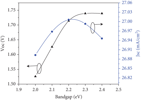
Figure 4 shows that FF and efficiency curve w.r.t. bandgap of P+ a-SiC layer. It has been noticed that the efficiency has a tremendous effect on bandgap of P+ a-SiC layer. As the bandgap increases, the efficiency increases and FF decreases. At 2.20 eV, the efficiency is the maximum. Beyond 2.20 eV, the efficiency sharply decreases. At 2.0 eV, 2.20 eV, and 2.4 eV, the FF are 0.803, 0.789, and 0.722, respectively, as well as the efficiencies are 32.951%, 36.52%, and 33.581%, respectively.

Figure 5 shows the Voc and Jsc curve w.r.t. bandgap of P+ a-SiC layer. Both the Jsc and open circuit voltage (Voc) are maximum at 2.2 eV. At 2.0 eV, 2.20 eV, and 2.4 eV, the open circuit voltages (Voc) are 1.526 V, 1.714 V, and 1.726 V, respectively, as well as the Jsc are 26.893 mA/cm2, 27.006 mA/cm2, and 26.946 mA/cm2, respectively. From the result, it has been observed that the optimum bandgap of P+ a-SiC layer is 2.2 eV.
5.1.3. Effect of Thickness of Intrinsic Layer
Figure 6 displays the FF and efficiency curve thickness of intrinsic layer. From the curve, it is depicted that the efficiency increases with increasing of thickness of intrinsic layer up to 8000 nm. Beyond 8000 nm of thickness, the efficiency decreases with increasing of thickness of intrinsic layer. That is why 8000 nm is the optimum thickness of intrinsic layer. Increase in thickness means more light absorption in this layer which leads to higher efficiency. It has been observed that the FF decreases with the increasing of thickness of intrinsic layer. At 6000 nm, 8000 nm, and 10000 nm of thickness of intrinsic layer, the fill factors are 0.819, 0.789, and 0.775, respectively, as well as the efficiencies are 36.217%, 36.52%, and 36.382%, respectively.

The Voc and Jsc curve w.r.t. thickness of intrinsic layer is shown in Figure 7. The Jsc increases with the increase of the thickness of intrinsic layer because more area surface and thickness means more short circuit current density. But the open circuit voltage (Voc) is constant (1.714 V). At 6000 nm, 8000 nm, and 10000 nm of thickness of intrinsic layer, the short circuit currents (Jsc) are 25.816 mA/cm2, 27.006 mA/cm2, and 27.379 mA/cm2, respectively. From the above result and discussion, it has been observed that the optimum thickness of intrinsic layer is 8000 nm.

5.1.4. Effect of Thickness of P+ a-SiC Layer
Figure 8 shows the FF and efficiency curve w.r.t. thickness of P+ a-SiC layer. At 15-20 nm of thickness, the efficiency is almost constant. Beyond that, the efficiency sharply decreases as the figure shows that. The fill factor decreases with increasing the thickness of P+ a-SiC layer. At 15 nm, 50 nm, and 100 nm thickness of P+ a-SiC, the fill factors are 0.789, 0.783, and 0.781, respectively, as well as efficiencies are 36.52%, 35.219%, and 33.819%, respectively.

Figure 9 shows the Voc and Jsc curve w.r.t. thickness of P+ a-SiC layer. The short circuit current density decreases with increasing the thickness of P+ a-SiC layer, but the open circuit voltage increases up to 50 nm. Beyond that, it decreases with increasing the thickness which has been observed in the simulation. At 15 nm of thickness, the open circuit voltage (Voc) is 1.714 V and the Jsc is 27.006 mA/cm2.

5.1.5. Effect of Thickness of n-Si Layer
Figure 10 shows the FF and efficiency curve w.r.t. thickness of n-Si layer. From the figure, it is depicted that the efficiency is almost constant at 15-100 nm of thickness of n-Si. Beyond 30 nm, the efficiency sharply decreases. So, the optimized thickness for n-Si layer is 15-30 nm at 15 nm of thickness, the FF is 0.789, and efficiency is 36.52%. The -axis is in log10 scale.
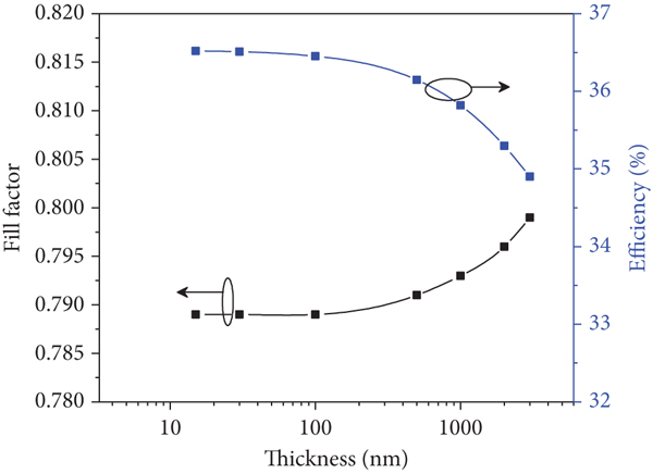
Figure 11 shows the Voc and Jsc curve w.r.t. thickness of n-Si layer. The Voc is almost same at 15-1000 nm, and after that, Jsc decreases sharply. The Jsc decreases with increasing the thickness of n-Si layer. The -axis is in log10 scale. From the simulation result, it has been noticed that the optimum thickness of n-Si layer is 15-100 nm.

5.1.6. Effect of Carrier Concentration
The carrier concentration has a great influence in the performance on HIT solar cell. Figure 12 shows FF and efficiency curve w.r.t. carrier concentration of P+ a-SiC layer curve. From the simulation, it has been observed that the efficiency is the maximum at the carrier concentration of 1e21 cm-3. So, the optimized carrier concentration is 1e21 cm-3. But the fill factor (FF) is the maximum at the carrier concentration of 1e19 cm-3. At 1e18 cm-3, 1e21 cm-3, and 1e22 cm-3 of carrier concentration, the fill factors are 0.742, 0.789, and 0.724, respectively, as well as efficiencies are 22.408%, 36.52%, and 35.799%, respectively. Here, the -axis is in log10 scale.

Figure 13 shows the Voc and Jsc curve w.r.t. carrier concentration of P+ a-SiC layer curve. Both the open circuit voltage and short circuit current increase with the increase of the carrier concentration of P+ a-SiC layer. The short circuit current density is almost constant after 1e21 cm-3 of carrier concentration. At 1e21 of carrier concentration, the open circuit voltage (Voc) is 1.714 V and the Jsc is 27.006 mA/cm2. Here, the -axis is in log10 scale. It has been observed that the optimum carrier concentration is 1e21 cm-3 as it shows the maximum efficiency.

5.1.7. Effect of Temperature
The temperature has a tremendous effect on HIT solar cell performance. Figure 14 shows the FF and efficiency curve w.r.t. temperature. It is depicted from the figure that the FF increases with increasing the temperature, but the efficiency increases sharply up to 330 K due to more breaks of bonding which helps to escape more electron, and after that, it is almost constant. At 270 K, 300 K, and 340 K of temperature, the fill factors are 0.765, 0.789, and 0.842, respectively, as well as the efficiencies are 33.609%, 36.52%, and 38.330%, respectively.

The short circuit current density and open circuit voltage also respond to the temperature variation. Figure 15 shows the Voc and Jsc curve w.r.t. temperature. It is clear from the figure that the open circuit voltage (Voc) decreases with increasing temperature due to decreasing Rsh, but the Jsc increases with increasing the temperature due to decreasing the series resistance (Rs). At 270 K, 300 K, and 340 K of temperature, the open circuit voltages are 1.725 V, 1.714 V, and 1.659 V, respectively, as well as the short circuit current densities are 25.461 mA/cm2, 27.006 mA/cm2, and 27.435 mA/cm2, respectively.

5.1.8. J-V and P-V Curve of Proposed HIT Model
Figure 16 shows the J-V and P-V curve of heterojunction with intrinsic layer (HIT). It has been observed that the optimum efficiency of 36.52% with open circuit voltage (Voc) is 1.714 V, FF is 0.789, and Jsc is 27.006 mA/cm2. The maximum power that has been observed is 36.52 mW/cm2.

5.2. Si-Based Heterojunction without Intrinsic Layer
The Si-based homojunction without intrinsic layer has a poor performance as well as efficiency. This is due to the less light absorption in the only P+ a-SiC layer and n-type Si layer. The simulation result without the intrinsic layer by varying thickness is given in Table 4.
The poor performance of the device without the intrinsic layer compared to the one with it (>36%) is primarily due to the intrinsic layer’s crucial role in a heterojunction solar cell. It mitigates carrier recombination, decreases the energy barrier for electron-hole separation, and reduces losses by improving the fill factor. These functions enhance charge separation, reduce recombination, and optimize electrical characteristics, significantly boosting efficiency compared to the reference device.
5.3. Heterojunction with Intrinsic, EBL, and Defects
In this simulation, the heterojunction solar cell with intrinsic layer, EBL, and defects has been simulated. It has been observed that Si-based heterojunction with EBL and defects has the efficiency less than the efficiency of Si-based heterojunction with and without EBL. The simulation result is V, mA/cm2, , and .
5.4. Comparison with Another Heterojunction Solar Cell
The comparison of heterojunction solar cell with other prepublished research work is given in Table 5.
6. Conclusion
In summary, this research is aimed at simulating the performance of a heterojunction with intrinsic thin layer (HIT) solar cell, and it has yielded promising results. The study identified optimal parameters for this HIT cell configuration, with key findings indicating that the ideal thicknesses for the P+ a-SiC layer, N+/I intrinsic layer, and n-Si layer are 15 nm, 8000 nm, and 15 nm, respectively. Additionally, the optimal bandgap values were determined to be 2.20 eV, 2.70 eV, and 1.12 eV for the P+ a-SiC, N+/I intrinsic layer, and n-Si layers, respectively. These optimizations led to an impressive peak efficiency of 36.52%, accompanied by an open circuit voltage (Voc) of 1.714 V, fill factor (FF) of 0.789, and short circuit current density (Jsc) of 27.006 mA/cm2. It is worth noting that further enhancements in efficiency may be achievable through careful control of band tail and band state parameters. These results lay the foundation for the potential fabrication and real-world implementation of such HIT solar cells in laboratory settings, aiming to validate and enhance the simulated performance for practical, high-efficiency photovoltaic applications.
Data Availability
The data supporting the investigation’s results are available upon reasonable request from the relevant author.
Conflicts of Interest
The authors declare that they have no conflicts of interest.
Acknowledgments
The authors would like to thank the Pennsylvania State University, USA, for providing them the Analysis of Microelectronic and Photonic Structures One-Dimensional (AMPS-1D) device simulation package.